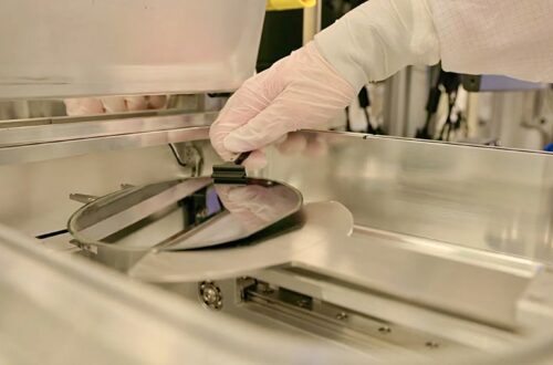
An on-device AI memory chip moved a step closer to reality this month. Engineers at the University of Southern California’s Viterbi School of Engineering, working under professor J. Joshua Yang, built an ultrathin switch. The switch could let a phone run a large AI model on its own, without sending anything to a cloud server.
Why the bottleneck is the selector, not the storage material
Their work does not target the part of a memory chip that stores data. It targets the part that decides which single cell in a memory grid gets to be read or written at any moment. That gatekeeper component is called a selector. Its limits, not the storage material sitting next to it, have kept engineers from packing memory as densely as modern AI workloads now demand.
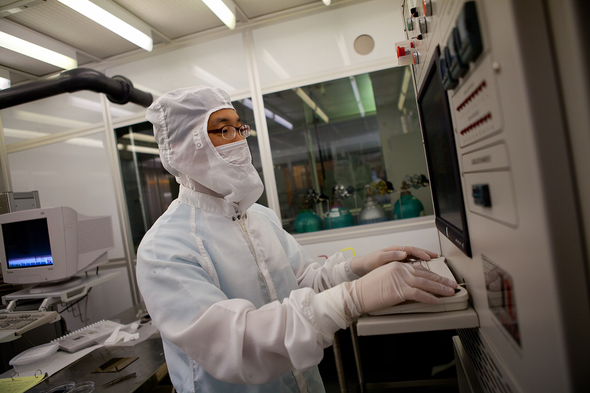
The new selector is built from five stacked atomic layers of two-dimensional materials: graphene, molybdenum disulfide, a tunnel barrier, molybdenum disulfide again, and graphene. In laboratory testing, it survived more than one trillion switching cycles. It also told an open state from a closed state roughly 100 times more reliably than the best selectors before it, according to the peer-reviewed paper published in Nature Electronics on September 12.
That combination of durability, precision, and thinness matters. It opens a path to stacking memory in three dimensions, something today’s transistor-based selectors cannot do.
On-device AI memory chip, why the bottleneck sits at the gate, not the storage
Professor Yang summarized the finding in USC’s own announcement: memory is the bottleneck for AI hardware, and the bottleneck for memory is not the memory device itself. It is its gatekeeper. That gatekeeper is the selector, and understanding why requires a look at how memory chips are wired.
How a selector works, in plain terms
Picture a memory chip as a grid of streets, with one storage cell parked at every intersection. To read or write a single cell, the chip has to reach that one intersection. It cannot disturb its neighbors on the same street while doing so. The part that opens or blocks traffic at each intersection is the selector. In plain terms, it is the switch that lets a chip talk to one memory cell at a time. Without it, the chip would have to address an entire row or column at once.
For decades, that switch has usually been a three-terminal transistor. Transistors work, but they are relatively large, and their flat structure makes them hard to stack in three dimensions. Every extra layer of memory built on top of a transistor-based selector adds size and heat. That is part of why phones and laptops cannot yet hold as much fast memory as a data center rack.
As AI models have grown, that constraint has turned into a hard ceiling. Running a large language model locally, entirely on a phone, means holding billions of parameters in memory. That memory has to be fast enough to keep up with the model’s calculations. Cloud data centers solve this by adding more memory chips and more power. A phone does not have that option; it has a fixed battery and a fixed amount of space inside its case.
That is the gap the USC team is trying to close. Instead of inventing a new way to store data, they focused on shrinking and strengthening the gatekeeper that decides which stored bit gets touched next.
Five atomic layers instead of a transistor
Their approach starts from different physics than a transistor altogether. It is built directly into the memory grid itself, and it is thin enough to stack in layers rather than spread across a flat surface.
On-device AI memory chip, five atomic layers replace a bulky switch
The USC selector is a five-layer stack: graphene on top, then molybdenum disulfide, then a tunnel barrier in the middle, then molybdenum disulfide again, then graphene on the bottom. Electric current has to tunnel through that middle barrier. The research team built two versions of it, one using hexagonal boron nitride and the other using gallium sulfide, to compare the tradeoffs each material offered.
The boron nitride version was the strongest performer on durability. It held a nonlinearity, the ratio that tells an “open” reading apart from a “closed” one, above ten million to one. It survived more than one trillion switching cycles in testing and switched in under 20 nanoseconds. It also barely changed behavior as temperature rose, a property ordinary transistor selectors tend to struggle with.
Two material tradeoffs: durability versus voltage
The gallium sulfide version traded some of that performance for something phones care about directly. It operates at just 2.5 volts, low enough to matter for battery life, with nonlinearity still above one million to one.

Both figures beat the previous best published results for this class of device by roughly two orders of magnitude, according to the paper. The uniformity mattered as much as the peak numbers. Because the barrier is built from stacked atomic layers rather than etched or deposited unevenly, cell-to-cell variation across a chip drops sharply. That variation is one of the things that has made earlier selector designs unreliable at scale.
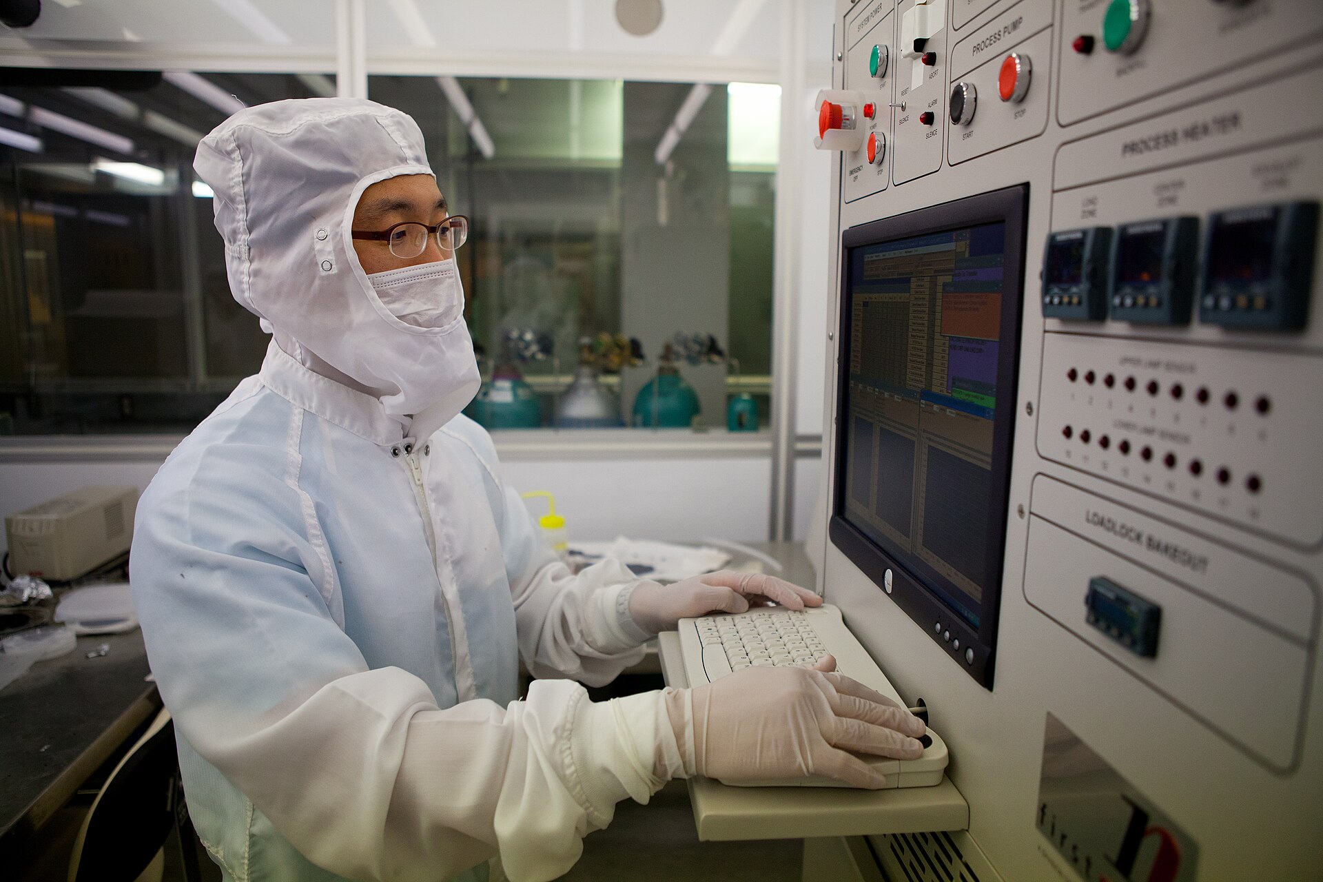
The project was led by USC in collaboration with the University of Florida, the Air Force Research Laboratory, the US Army Research Laboratory, and Japan’s National Institute for Materials Science. It appears in Nature Electronics under the title “High-performance tunnel-junction selectors with graded tunnel barriers based on five-layer van der Waals heterostructures.”
Lab results and what still needs to be proven
Other corners of the chip industry are attacking the same memory bottleneck from a different direction. Cerebras, for one, keeps an entire AI model’s memory on a single uncut wafer instead of redesigning the switch inside each cell. The USC group’s own peer-reviewed paper lays out the full device physics behind their approach.
What this result does not settle yet
A laboratory demonstration of a single selector device is not the same as a finished memory chip. To matter for phones, selectors like this one still need to be paired at scale with actual storage elements, such as a resistive memory cell or a capacitor. They also need to be manufactured across a full wafer rather than tested as a handful of devices on a bench.
The paper’s own authors flag that gap directly. It presents selector-resistor and selector-capacitor integration as a future direction, not a demonstrated one. It also notes that the feasibility of large-scale fabrication still needs further study.
How far this still is from a shipping product
No phone maker or memory manufacturer has announced plans to build this specific device into a product. Academic selector research has a long history of strong lab numbers. Those numbers often take years to reach a factory floor, if they reach one at all. The transistor-based selectors phones use today went through that same multi-year path from paper to production.
DRAM, NAND flash, and newer high-bandwidth memory remain the technologies actually shipping in phones and data centers. They will keep shipping while this approach, and several competing ones, work through the manufacturing questions the paper leaves open.
What the result does establish is that the physics works. A five-layer stack this thin can match or beat the electrical performance of a selector many times its size. If that holds up at manufacturing scale, the benefit would not stop at phones. The same memory bottleneck limits how much AI a single data center rack can serve per watt. A smaller, cheaper gatekeeper would matter there too.
References
References
USC Viterbi School of Engineering, “A Tiny Gatekeeper Could Keep AI on Your Device,” September 21, 2026
Liu et al., “High-performance tunnel-junction selectors with graded tunnel barriers based on five-layer van der Waals heterostructures,” Nature Electronics, September 12, 2026