
SK Hynix Intel talks, first reported by Reuters on September 16, would put Korean memory production on American soil for the first time. The two companies have discussed manufacturing RAM chips in the United States, according to people the agency did not name.
Two arrangements were described. One would have SK Hynix lease space inside the factory Intel is building in Ohio. The other is a joint venture that could bring in cloud service providers as partners.
SK Hynix has not confirmed either. In a statement to TechCrunch the company said it is exploring various options to strengthen its global competitiveness but that no specific plans or arrangements have been finalized, and that no decisions have been made on the two scenarios described.
What makes the report worth reading carefully is not the deal itself, which may never happen, but what it says about where memory is made and why that has suddenly become a question.
SK Hynix Intel, and what was actually reported
The distinction between leasing and a joint venture is not a detail. Leasing space means SK Hynix installs and runs its own tools inside a building Intel owns, keeping its process to itself.
A joint venture is a shared company with shared decisions, and the mention of cloud providers points at the customers who are short of memory rather than at a chipmaker.
Neither option is the same as the plant SK Hynix is already building in the United States. The 3.8 billion dollar facility in West Lafayette, Indiana, is an advanced packaging and research site, with mass production expected to begin in 2029.
Packaging is the back end of the process. Under the Indiana plan, DRAM wafers are made in South Korea and then stacked and finished in Indiana into high-bandwidth memory for AI accelerators.
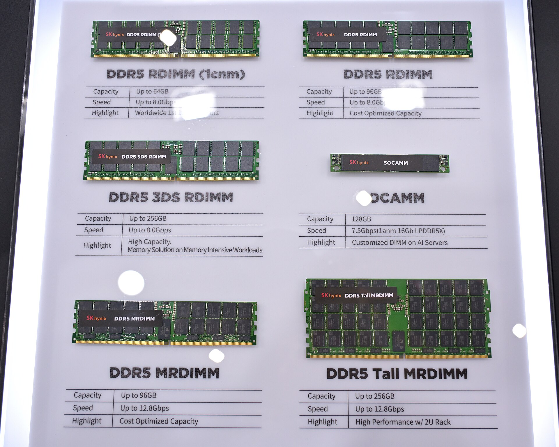
An Ohio arrangement would move the front end, the wafer fabrication itself. That is the step the company has never done outside Korea, and the report does not say which memory types would be made there.
The two companies have transacted before. Intel sold its NAND flash business to SK Hynix in 2020 for 9 billion dollars, a deal that gave the Korean company a manufacturing site in Dalian, China.
SK Hynix Intel options, why Ohio and why now
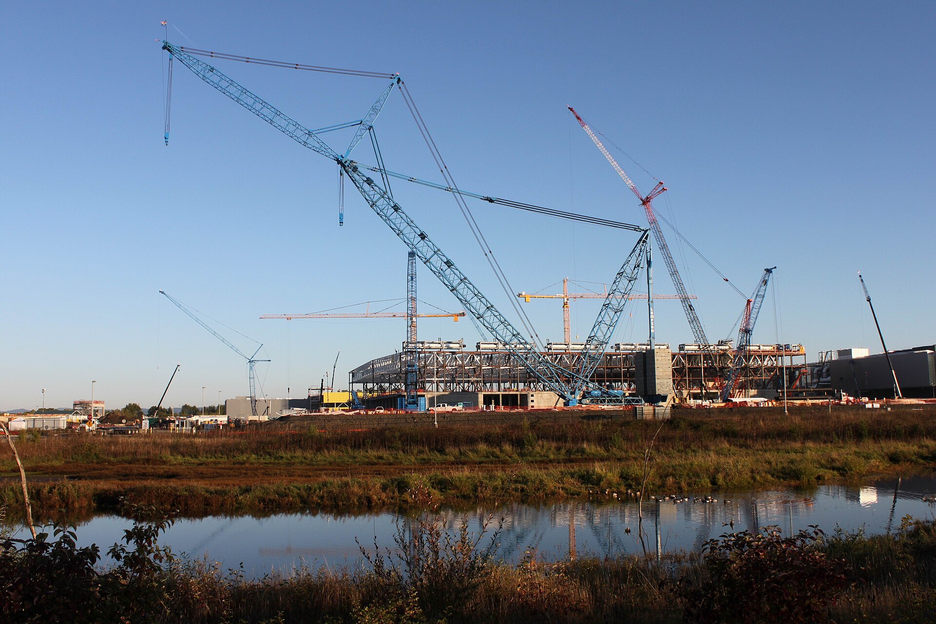
Intel has floor space in Ohio because it has not filled it. The New Albany campus is a 28 billion dollar project covering 2.5 million square feet, of which 600,000 square feet is cleanroom.
It is also very late. Production was originally promised for 2025, pushed to 2027, and now sits at 2030 or 2031 for the first fab, with a second building following in 2032.
Chief executive Lip-Bu Tan slowed the construction deliberately, saying the company had invested too much too soon and wanting capital spending matched to actual customer orders.

On the memory side the pressure runs the other way. Capacity has been reallocated toward high-bandwidth memory for AI systems, conventional DRAM contract prices are still climbing quarter after quarter, and analysts do not expect meaningful new capacity before late 2027.
Policy is pushing in the same direction. The White House said in January that it could impose broader tariffs on imported semiconductors while offering relief to companies investing in domestic manufacturing.
SK has signalled openness to that. Group chairman Chey Tae-won said in July that the company should build plants in the United States if feasible, alongside those in Korea, and the same month SK Hynix listed American depositary receipts on Nasdaq, raising 26.5 billion dollars in the largest foreign listing in US history.
The customers are the third force. The AI buildout that is reshaping American energy demand is the same buildout consuming memory, and a joint venture including cloud providers would be those buyers paying to secure supply rather than bidding for it.
What has not been decided
The report rests on unnamed sources, and the company named in it has publicly said no decision exists. Intel did not comment. Nothing here is a signed arrangement.
Even if it is signed, the technical work is not trivial. A logic fab and a memory fab are not interchangeable buildings; tool sets, layout and process chemistry differ, and moving a DRAM node into a shell designed for Intel logic would take its own qualification programme.
The timing is awkward too. Ohio output is not scheduled until 2030 at the earliest, which is well past the window in which the current shortage is expected to resolve.
There is a regulatory step at home as well. Seoul treats the decision as the company’s to make, but any plan involving strategically important chip technology can trigger a government review under Korean law designed to prevent sensitive technology from moving overseas.
What can be said now is narrow. A Korean memory maker is publicly weighing American wafer fabrication for the first time, an American logic maker has unused capacity it cannot yet fill, and the buyers of both have more cash than supply.
References
TechCrunch, SK Hynix reportedly in talks with Intel to build memory chips in US, September 16, 2026 · SK Hynix Newsroom statement · Construction Dive, Intel delays Ohio chip project again · TechCrunch, SK Hynix raises $26.5B in the biggest foreign IPO in US history


