For most of the last decade, the story of the AI boom has been told through GPUs — how many a company can buy, how fast they can be linked together, how much power they draw. Increasingly, though, engineers building AI systems say the real bottleneck isn’t the processor doing the thinking. It’s the memory struggling to feed it fast enough.
The problem has a name in the chip industry: the memory wall. As AI models grow larger and their context windows stretch longer, the “working memory” a system needs to hold close to the processor — the key-value cache that lets a chatbot remember what it just said, for instance — grows right along with it. Keeping all of that data in the fastest available memory, DRAM, is expensive and power-hungry. Pushing it out to cheaper, denser storage means waiting for it to come back, and that round trip is what slows an AI system down.

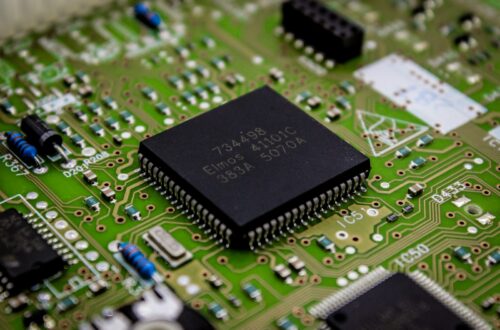
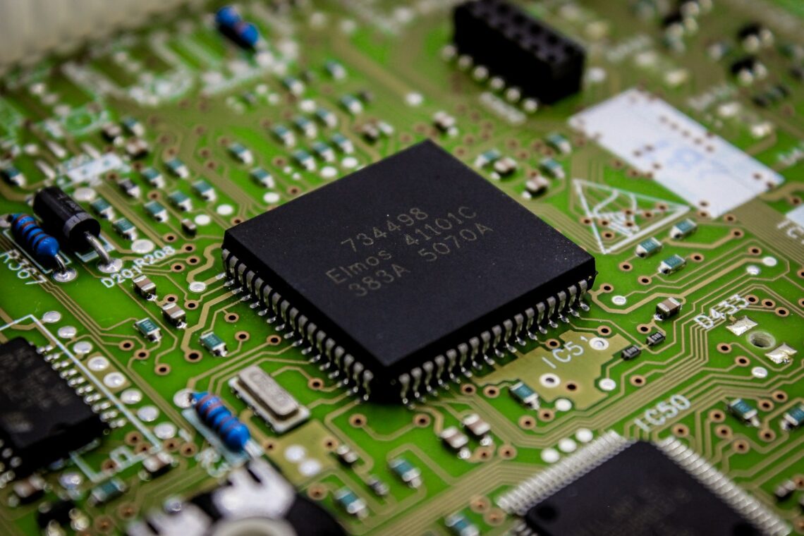
Photo: Bermix Studio / Unsplash (free license)
A useful way to picture the setup inside most of today’s computers is a worker with a small desk and a large warehouse down the hall. DRAM is the desk: blisteringly fast to reach into, but limited in size and it forgets everything the moment the power goes out. NAND flash, the technology behind SSDs, is the warehouse: enormous capacity, and it remembers its contents indefinitely, but every trip to fetch something adds real, measurable delay. Modern AI inference increasingly needs to make that trip to the warehouse, again and again, at massive scale.
A team at the University of Seoul has proposed one of the more direct attempts yet to close that gap. In a paper published in July in the journal IEEE Access, researchers S. Kim, J.-H. Ahn, M. Koo, and Y. Kim describe a hybrid memory device they call NAD — short for NAND-and-DRAM — that tightly integrates the two technologies at the device level rather than simply placing them side by side on a circuit board. The key innovation is architectural: NAD eliminates the intermediate I/O buffers and data buses that conventional systems use to shuttle data between DRAM and NAND flash, allowing direct, parallel transfer between the two instead. In the desk-and-warehouse picture, it’s less like building a faster hallway and more like tearing down the wall between the rooms.
The University of Seoul’s approach is one of several the memory industry is racing to develop in parallel, and comparing them says something about how differently engineers are attacking the same wall. SK hynix has proposed a concept it calls H3, which pairs conventional High Bandwidth Memory with what it calls High Bandwidth Flash — stacks of 3D NAND dies built and packaged the same way HBM is — sitting on the same interposer next to the GPU. The idea is to give AI accelerators a large, flash-based capacity tier without forcing every request to leave the package entirely, though flash’s slower access speed and limited rewrite endurance, often only around 100,000 cycles, remain real constraints.
Belgium’s imec research institute, meanwhile, has taken a more physically radical approach: a prototype 3D memory structure that borrows charge-transfer principles from decades-old camera-sensor technology, built from indium gallium zinc oxide to reduce current leakage and allow denser vertical stacking of memory layers. Imec has demonstrated charge transfer above 4 MHz in early testing, though the institute is candid that this remains a lab prototype, with real questions still open about heat management, layer scaling, and manufacturability.
Set against those approaches, the University of Seoul’s contribution is notable for being the most conceptually minimal: rather than stacking flash and DRAM in new package geometries, NAD tries to make the two kinds of memory behave, electrically, as close to a single device as the underlying materials will allow. Whether that direct-integration approach proves more practical to manufacture than interposer-based or 3D-stacked alternatives is a question the paper’s authors don’t fully resolve — as an IEEE Access publication, NAD remains squarely a research proposal rather than a product roadmap, and the paper does not claim a path to near-term commercial production.
The stakes for solving this problem reach well beyond data centers. The same DRAM and NAND flash supply chains that feed AI accelerators also feed ordinary laptops, phones, and game consoles, and industry analysts have already coined the term “RAMageddon” to describe a market where AI infrastructure demand is beginning to squeeze the physical supply of memory chips available for everything else. A memory architecture that delivers more effective bandwidth and capacity per chip — without simply demanding more raw material — is one of the few paths that could ease that squeeze from the inside, rather than by building more factories.
None of these hybrid approaches, from Seoul, from SK hynix, or from imec, is close to shipping in a commercial chip today. But the fact that a university lab, a leading memory manufacturer, and an independent European research institute have converged on the same basic idea — stop treating fast memory and dense memory as two separate rooms — suggests the industry has decided the memory wall is no longer something GPU horsepower alone can out-run.
Sources: IEEE Access, vol. 14, pp. 106983-106994, 2026 (DOI: 10.1109/ACCESS.2026.3710576); Semiconductor Engineering (July 29, 2026); SemiWiki, TechRadar Pro, Startup Fortune coverage of SK hynix H3 and imec 3D memory prototypes.