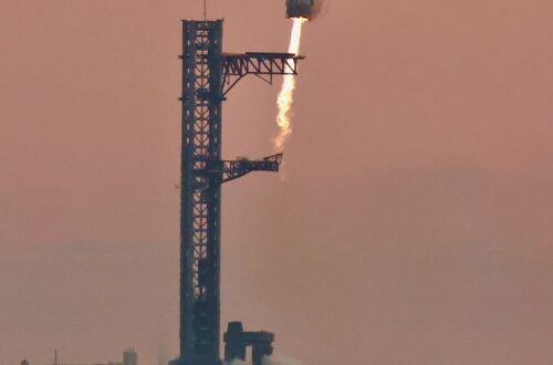
When Elon Musk answered a question about the Terafab renderings with three words earlier this year, the exchange read as provocation. Free Electron Laser For The Win was a slogan about a machine nobody had built for the purpose, aimed at a monopoly nobody had dented.
Six months on, the argument has left the timeline and turned into hardware, money and a schedule. On June 2 the US Department of Commerce and NIST signed a final award of 150 million dollars to a Silicon Valley startup called xLight, specifically to build and demonstrate a first-of-its-kind free-electron laser as an extreme ultraviolet light source.
What makes this moment worth revisiting is not that the challenger got funded. It is that the incumbent answered in the same window, and the two answers are now aimed at the same year.
The Money Arrived Before the Light Did
xLight signed a letter of intent with Commerce on December 2, 2025, and the award was finalised six months later. The structure is unusual: the department takes 150 million dollars of equity in the company, making a federal agency a shareholder in a pre-revenue accelerator startup.
That is not unprecedented any more. In August 2025 the federal government agreed to an 8.9 billion dollar ownership stake in Intel, on top of the 5.7 billion in CHIPS funds Intel had already received. The state has started taking positions rather than writing grants.
The prototype will be built at the Albany NanoTech Complex in New York, the flagship CHIPS research site that opened in July 2025 as the National Semiconductor Technology Center. The location is the point: the campus already houses the CHIPS for America EUV Accelerator, including a standard high-numerical-aperture EUV scanner.
A light source is useless without something to shine into. Putting the prototype next to a working High-NA tool means xLight can attempt the only demonstration that would actually settle the question, which is exposing wafers rather than publishing beam parameters.
Chief executive and chief technology officer Nicholas Kelez has said the facility’s lithography capability is what will enable the research, and the company is targeting 2028 for the prototype to operate there.
The company has also assembled the kind of board that changes how procurement officers read a pitch deck. In March former Intel chief executive Pat Gelsinger joined xLight as executive chairman, and in the same month became a partner at Playground Global, the venture firm that then led a 40 million dollar Series B in July.
The engineering is being borrowed rather than invented from scratch. xLight is drawing on Fermilab for superconducting radio-frequency cavities and cryomodules, and on Cornell to commercialise work from the CBETA energy-recovery accelerator, while continuing to work across the Department of Energy national laboratory system.
Its central claim is a number and a topology. The company says its source can deliver roughly four times the EUV output of a conventional laser-produced plasma system, and that one unit can feed several scanners rather than each scanner carrying its own source.
The Incumbent Did Not Stand Still
The case for a free-electron laser has always rested on one accusation: that ASML’s method of making extreme ultraviolet light is brutally inefficient, and that the inefficiency caps how many wafers a scanner can expose in an hour.
ASML’s answer this year was to attack the cap directly. The company demonstrated a proof of concept running its source at 1,000 watts, against roughly 600 watts as an average figure in the field today.
Getting there meant changing the choreography inside the vessel. The droplet rate was doubled to around 100,000 tin droplets per second, and the single main laser pulse gave way to a sequence.
A one-micron pre-pulse flattens the droplet, a second one-micron pulse rarefies it, and only then does the ten-micron carbon dioxide main pulse arrive to turn the thinned target into plasma. It is the same physical principle, executed with far more finesse.
The throughput arithmetic is what matters commercially. ASML has framed the goal as roughly halving wafer processing time by 2030, moving from about 220 wafers per hour today to around 330, with 400 to 500 seen as where the architecture eventually lands.
The company has also been unusually plain about headroom, describing a reasonably clear path to 1,500 watts and saying it sees no fundamental reason it could not reach 2,000. That is a direct rebuttal to the premise that LPP is near a wall.
None of this makes the underlying objection false. Tin debris still degrades the collector mirror, the hydrogen flow used to keep that mirror clean is still measured in hundreds of litres a minute, and doubling the droplet rate makes the contamination problem harder rather than easier.
What ASML has done is outrun the objection rather than resolve it, and it is worth remembering the company examined free-electron lasers twice, roughly a decade ago and again more recently, and chose the lower-risk road both times.
So the competitive question has changed shape. It is no longer whether a cleaner, more efficient source would be better in principle, but whether a source that has never lased at 13.5 nanometres can arrive before the incumbent closes the gap that justified building it.
Why the Terafab Site Announcement Matters to a Physics Problem
A free-electron laser only makes economic sense as shared infrastructure. One accelerator feeding a beamline that splits to perhaps eight or ten scanners is cheap per tool; the same accelerator feeding two scanners is an expensive way to buy light.
That is why the concept keeps reappearing alongside very large fabs, and why the Terafab news of the last few months is more relevant to xLight than anything Musk typed.
Musk announced the project on March 21, and on August 6 Tesla and SpaceX confirmed the site: Grimes County, Texas, with a first phase put at more than 16.8 billion dollars. Earlier filings and reporting had sketched an initial commitment near 55 billion and a total buildout that could approach 119 billion.
The stated scale is what makes the light-source question live. Terafab is described as targeting on the order of one million wafer starts per month, with Musk framing the output in compute terms rather than chip terms, and the venture intends to keep design, lithography, fabrication, memory, packaging and test on one site.
At that density, the tool count runs into the hundreds, and the cost of giving every one of them its own multi-hundred-kilowatt source stops being a rounding error. This is the only regime in which the central-power-station model beats the per-tool model on total cost of ownership.
The obstacles are still exactly where they were, and they are not small. No free-electron laser has yet produced light at 13.5 nanometres for lithography.
Japan’s High Energy Accelerator Research Organization, which has pushed an energy-recovery linac approach furthest, demonstrated spontaneous emission at around 20 micrometres with a 17 mega-electronvolt beam; reaching EUV requires an accelerator closer to 800 mega-electronvolts, which does not exist yet.
Cost estimates for a new accelerator of that class have been put in the range of 260 to 400 million dollars, and the precision beam distribution system that would carry light to a row of scanners without ruinous loss is not a product anyone sells.
There is also a scheduling truth that no amount of enthusiasm changes. A fab cannot wait on a science programme, so the first Terafab phase will run on the tools that exist, which means ASML scanners regardless of what the long-term architecture becomes.
The genuinely new thing this year is that two clocks now point at the same number. xLight is aiming to have its prototype running at Albany in 2028, and Terafab is aiming at mass production in 2028.
That coincidence is what turns a three-word post into a procurement question. If the prototype lases at the right wavelength on schedule, someone will have to decide whether the second phase of the largest fab ever proposed is designed around a light source that did not exist when the first phase broke ground.
References
- NIST and US Department of Commerce, “Department of Commerce Announces Finalization of CHIPS Incentives with xLight to Support Next-Generation Light Source for Lithography,” June 2, 2026.
- Sara Samora, “XLight, Commerce Department finalize 150M CHIPS Act award,” Manufacturing Dive, published December 2, 2025, updated June 2, 2026.
- Reporting on xLight’s 40 million dollar Series B (Playground Global) and Pat Gelsinger’s appointment as executive chairman, March and July 2026.
- Coverage of ASML’s 1,000 W EUV source proof of concept and 2030 throughput roadmap, Tom’s Hardware and Bits and Chips, 2026.
- Terafab site confirmation, Grimes County, Texas, Electrek, August 6, 2026; project announcement, March 21, 2026.
- KEK energy-recovery linac FEL programme materials; Fermilab superconducting RF and Cornell CBETA collaboration disclosures.
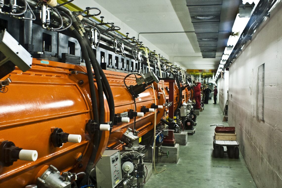
- Featured image: CERN Linac, Florian Hirzinger, Wikimedia Commons, CC BY-SA 3.0.